
Introduction TO Bipolar Junction Transistor
The transistor is a solid- state device whose operation depends upon the flow of electric charge carries within the solid. A transistor consists of two P-N junctions formed by sandwiching either P-type or N-type semiconductor between a pair of opposite types. Accordingly, there are two types of transistors, namely:
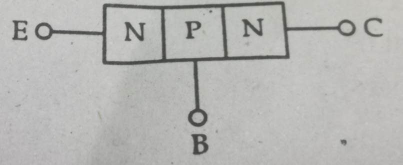
1. N-P-N transistor
2. P-N-P transistor
A N-P-N transistor is compared of two N-type semiconductors separated by a thin section of P-type as shown in the figure below.
However, a P-N-P transistor is formed by two P-sections separated by a thin section of N-type.
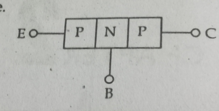
Each type of transistor has two P-N junctions-one junction between the emitter and base called emitter-base junction or simply the emitter junction and the other junction between the base and collector called the collector-base junction or simply the collector junction. Thus, a transistor is like two P-N junction diodes connected back to back. The two junctions give rise to three regions provided with three terminals called the emitter, base and collector.
Transistor Terminals
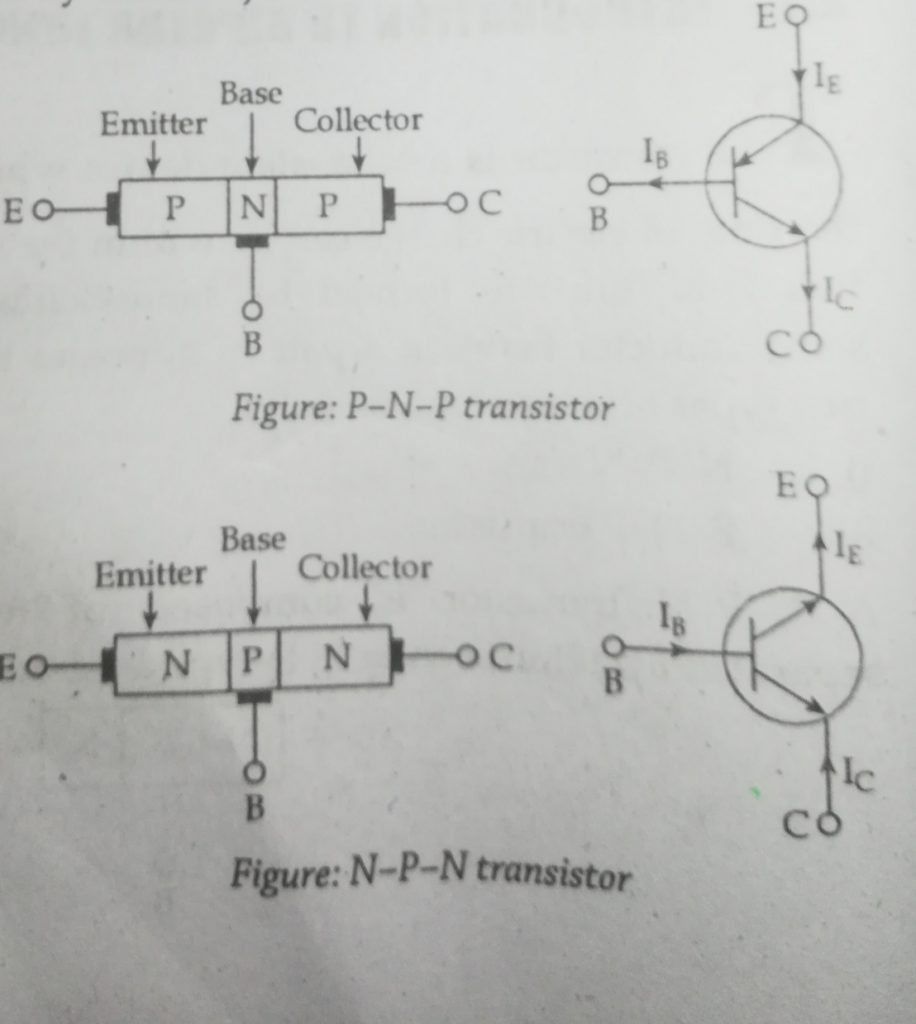
- Emitter
Its main function is to supply majority charge carriers (electrons in case of NPN transistors and holes in case of PNP transistors) to the base. The emitter is always forward biased with respect to base so that it is able to supply majority charge carries to the base. The emitter is heavily doped so that it may be able to inject a large number of charge carriers. It is of moderate size in order to maintain heavy doping without diluting it or mesh formation in it.
- Collector
It is the right hand section of the transistor and its main function is to collect majority charge carriers. Collector is always reverse biased so as to remove the charge carriers away from its junction with the base. It is large in size to withstand the temperature generated at the collector and is moderately doped.
- Base
It is the middle section of the transistor and is very lightly doped to reduce the recombination within the base so as to increase collector current and is very thin in comparison to either emitter or collector so that it may pass most of the injected charge carriers to the collector.
Current Flow Mechanism In NPN and PNP Transistor
- Current Flow Mechanism In NPN Transistor:
Figure below shows the NPN transistor with forward bias to emitter base junction and reverse bias to collector base junction. The forward bias causes the electrons in the N-type emitter to flow towards the bias.
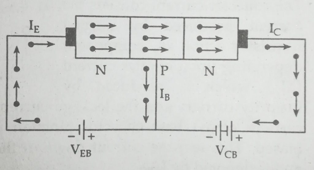
This constitutes the emitter current IE. As these electrons flow through the P-type base, they tend to combine with holes. As the base is lightly doped and very thin, therefore only a few electrons combine with holes to constitute base current IB. The remainder electrons cross over into the collector region to constitute collector current Ic. In this way, almost the entire emitter current flows in the collector circuit. It is clear that emitter current is the sum of collector and base currents I.e. IE=IB+IC.
In actual practice, a very little current (a few μA) would flow in the collector current. This is called collector cut off current and is due to minority carriers.
- Current Flow Mechanism In PNP Transistor
Figure below shows the basic component of a PNP transistor.
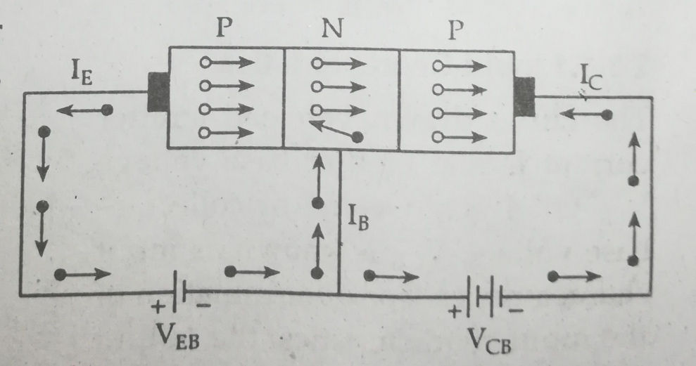
This constitutes the emitter current IE. As these holes cross into N-type base, they tend to combine with the electrons. As the base is lightly doped and very thin, therefore, only a few holes combine with electrons. The remainder cross into the collector region to constitute collector current IC. In this way, almost the entire emitter current flows in the collector circuit. It may be noted that current conducting within PNP transistor is by holes. However, in the external connecting wires, the current is still by electrons.
Input And Output Characteristics Of CB And CE Transistor
A. Common Base (CB) Configuration
In common base configuration, input is connected between emitter and base and output is taken across collector and base. Thus, base is common between input and output circuits.
In this arrangement, the emitter- base junction is forward biased and collector- base junction is reversed biased. This emitter current IE flows in the input circuit and collector current IC in the output circuit.
The ratio of collector current, IC to the emitter current, IE is called current amplification factor, α.
The collector current consists the current produced by normal transistor action i.e. component depending upon emitter current (αIE) which is produced by majority carriers and the leakage current due to movement of minority carriers across base-collector junction on account of it being reverse biased. This leakage current flows in the same direction as that of ICBO and is denoted by ICBO.
∴ Total collector current (IC) = αIE+ ICBO
The current ICBO sometimes referred to as ICO, is usually very small and may be neglected intransistor
calculation.
So,
α = ( IC – ICO)/ IE = IC / IE
Neglecting ICO in comparison with IC; we have,
IB=IE-IC = IE– (αIE+ ICBO) = ( 1 – α) * IE – ICO [∴ IC = αIE+ ICBO]
1. Input Characteristics

The curve drawn between emitter current IE and emitter base voltage VEB for a given value of collector base voltage VCB is known as input characteristics. For determination of the input characteristics, the output voltage VCB is maintained constant and the input voltage VEB is set at several convenient levels. Figure shows the input characteristics of a typical transistor in CB arrangement.
The following points can be noted from these characteristics:
- Emitter current , IE increases rapidly with small increase in emitter base voltage VEB. It means that input resistance is very small.
- The emitter current is almost independent of collector base voltage VCB. This leads to the conclusion that emitter current is almost independent of collector voltage.
Input resistance = (Change in emitter – Base voltage)/( Change in emitter current)
∴ ri = ▲VEB / ▲IE
As a very small VEB is sufficient to produce a large flow os emitter current IE, therfore input resistance is quite small of the order of a few ohms.
2. Output Characteristics
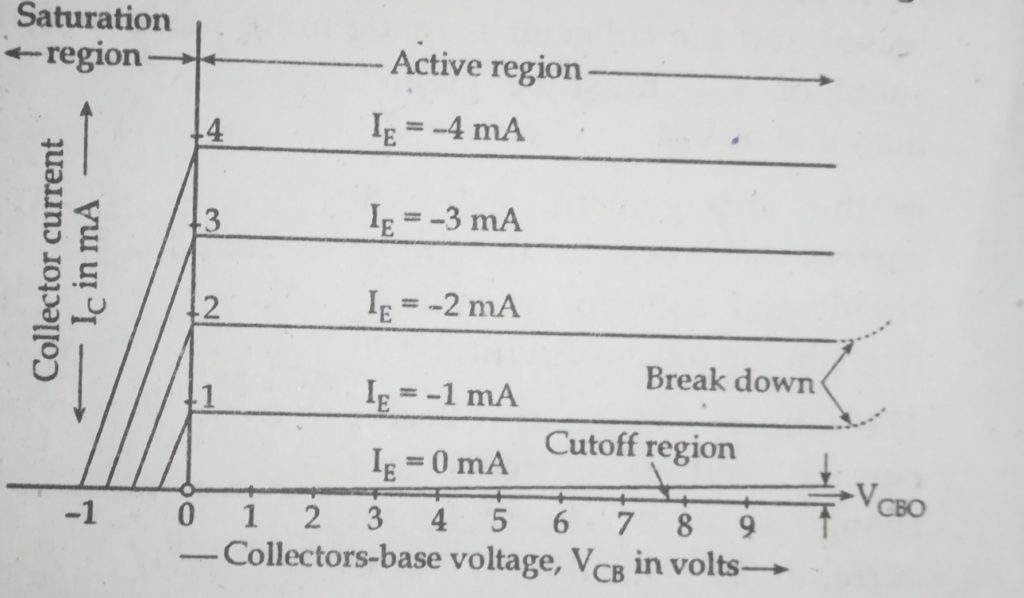
The curve drawn between collector current IC and collector-base voltage VCB for a given value of emitter current IE is known as output characteristics.
For determination of output characteristics, the emitter current is held constant at each of several fixed levels. Figure aside shows the output characteristics of a typical transistor in CB arrangement.
The noteworthy points regarding output characteristics of common base configuration are given below:
- The collector current IC varies with VCB only for very low voltage but transistor is never operated in this region.
- In cutoff region (emitter and collector junctions forward biased) small collector current IC flow even when emitter current IE = 0. This is the collector leakage current ICBO or ICO.
- In active region ( emitter forward biased and collector reverse biased) collector current IC is almost equal to IE and appears to remain constant when VCB is increased. In fact , there is very small increase in IC with increase in VCB. This is because the increase in VCB expands the collector- base depletion region and thus shortens the distance between the two depletion regions. Transistor is normally operated in this active region.
- A very large change in collector voltage causes a very small change in collector current I.e. output resistance of CB configuration is very high-the dynamic output resistance rout being given as the ratio of ▲VCB and ▲IC for a given value of IE.
I.e. r0 = ▲VCB / ▲IC at constant IE
- In saturation region ( both emitter and collector junction forward biased) collector current IC flows even when VCB = 0. Collector current IC is reduced to zero when VCB is increased negatively.
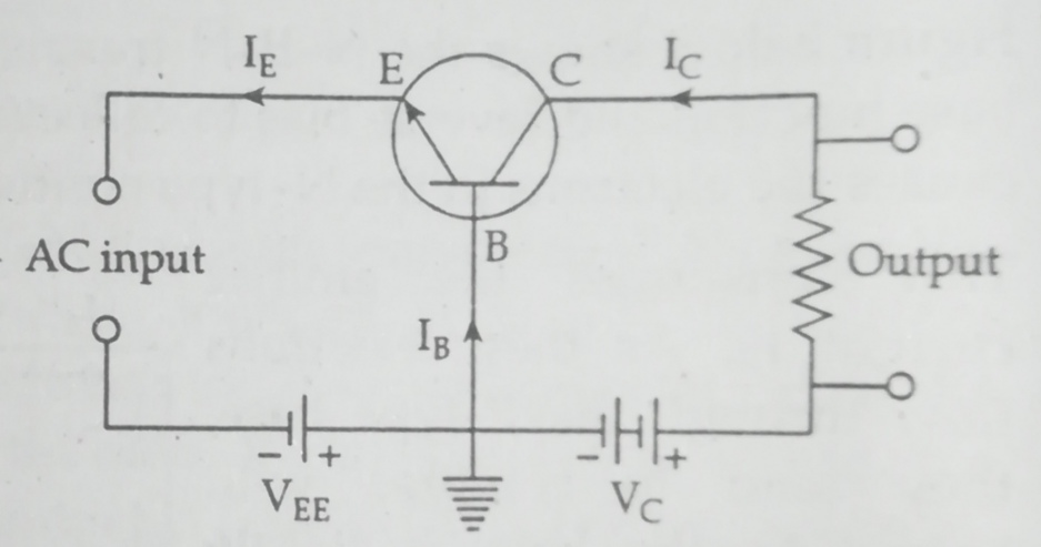
B. Common Emitter (CE) Configuration
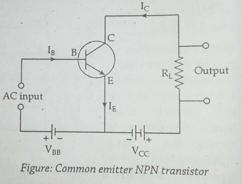
In common emitter configuration, input is connected between base and emitter while the output is taken between collector and emitter. Thus, emitter is common to input and output circuits. In this configuration, the bias voltage are applied between collector and emitter and base and emitter. Emitter-base junction is forward biased and the base is made more positive than the emitter by VBB, collector emitter junction is reverse biased and the collector is made more positive than emitter by VCC. The value of VCC must be greater than that of VBB.
In this arrangement, the base current IB flows in the input circuit and collector current IC flows in the output circuit.
The ratio of change in collector current (output current) and change in base current (input current) is called the base current amplification factor, β.
Also,
β = IC / IB = IC / (IE – IC) = (IC / IE) / (1- IC/ IE) = α / ( 1- α)
In CE configuration, a small collector current flows even when base current is zero. This is the collector cutoff current and denoted by ICEO. ICEO must be larger than ICBO. The current equations are:
IE = IB + IC
And,
IC = αIE + ICBO = α(IB + IC) + ICBO
Or, IC(1- α ) = αIB + ICBO
Or, IC = {α/(1- α) } * IB + ICBO/ (1- α) ———–(1)
And,
Total collector current,(IC) = βIB + ICEO —————(2)
Comparing equation (1) and (2); we have,(1
β = α / ( 1- α)
And,
ICEO = {α /(1- α) } * ICBO
Putting the value of ICEO = {α /(1- α) } * ICBO in the equation (2); we have
IC = βIB + {α /(1- α) } * ICBO
Or, IC = βIB + (1+β ) * ICBO
1. Input Characteristics
The curve drawn between base current IB and base-emitter voltage VBE for a given value of collector- emitter voltage VCE is known as the input characteristics. For determiantion of input characteristics, collector emitter voltage VCE is held constant and base current iB is recorded for different values of base-emitter voltage VBE.
The noteworthy points regarding input characteristics are given below:
- The input characteristics of CE transistors are quite similar to those of a forward biased diode because the base-emitter region of the transistor is a diode and it is forward biased.
- In comparison to common base arrangement base current increases less rapidly with the increases less rapidly with the increase base- emitter voltage, VBE. This indicates that input resistance is larger in common emitter configuration that in common base configuration. Due to initial non-linearity of the curve, input resistance varies from point to point in the initial part of the characteristics. Its value over the linear part of the curve is of the order of few hundred ohms.
- An increment in value of VCE causes the input current IB to be lower for a given level of VBE. This is because the higher levels of VCE provide greater collector-base junction reverse bias causing depletion region penetration into the base and thus reducing the distance between the collector- base and emitter-base regions. As a resuilt, more of the charge carriers from the emitter flows across the collector-base junction, and few flow out across the base lead.
The ratio of change in base-emitter voltage to the resulting change in base current at constant collector-emitter voltage is known as dynamic input resistance.
I.e. rin = ▲VBE / ▲IB at constant VCE
2. Output Characteristics

Output characteristics for a common emitter transistor in the curve drawn between collector current IC and collector- emitter voltage VCE for a given value of base current IB.
The noteworthy points regarding output characteristics are given below:
- The collector current IC varies with VCE for VCE between 0 to 1 V and then become almost constant and independent of VCE . The transistor are always operate above 1V.
- Output characteristics in CE configuration has same slope while CB configuration has almost horizontal characteristics. This indicates the output reistance in case of CE configuration is less than in CB configuration.
- Moderate output to input impedence ratio makes this configuration an ideal one for coupling between various transistor stages.
- With low values ( ideally zero) or VCE, the transistor is said to be operated in saturation region and in this region base current IB does not cause a corresponding change in collector current IC.
- With much higher VCE, the collector-base junction completely breaks down and because of this avalanche breakdown collector current IC increases rapidly and the transistor gets damaged.
- In cutoff region, small amount of collector current IC flows even when base current IB = 0. This is called ICEO. Since, main current IC is zero, the transistor is said to be cutoff.
The ratio of change in collector-emitter voltage to the change in collector current at constant base current is known as dynamic output resistance. It is calculated as the reciprocal of the slope of output characteristic at a given VCE.
i.e. rout = ▲VBE / ▲IC at constant IB
DC current gain, (β) = IC / IB
AC current gain, (β0) = ▲IC / ▲IB at constant VCE
Reference 1 : A reference book basic electronics engineering , Er. Sanjaya Chauwal, G.L Book house Pvt.Ltd.